Flip chip reflow soldering is a chip that can be directly connected to a ceramic substrate without soldering wires. We call it the DA chip.
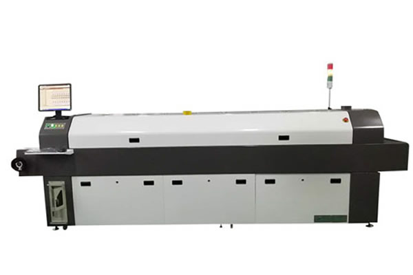
The current flip chip reflow soldering is different from the early flip chip that needs to be transferred to a silicon or other material substrate with a wire. The traditional flip chip is connected to the substrate with a bonding wire on the front side, and the flip chip is on the face The next is equivalent to subverting traditional chips. Jinlida focuses on the research of flip chip reflow soldering equipment.
Flip chip reflow characteristics
In fact, flip chip has a long history, parallel to vertical and horizontal structures. Its luminous property is that the active layer is downward, and the transparent sapphire layer is above the active layer. The light from the active layer needs to pass through the sapphire substrate to reach the outside of the chip.
Advantages of flip chip reflow soldering
1. Good heat dissipation performance. Since the active layer of the flip chip is close to the substrate, the heat flow path from the heat source to the substrate is shortened, and the thermal resistance of the flip chip is low, so the performance of the flip chip from light to thermal stability is hardly reduced.
2. In terms of luminous performance, under high current drive, the luminous efficiency is higher. Flip chip has good current spreading performance and ohmic contact performance. The voltage drop of flip-chips is generally lower than that of traditional chips and vertical chips, which makes flip-chips have great advantages in high-current driving, showing higher light efficiency.
3. Under high power conditions, flip chip is safer and more reliable than front mounted chip. In the device, especially in the high-power lens package (except for the traditional anti-lumen structure with protective shell), more than half of the dead light is related to the damage of the gold wire.
4. Smaller size, lower product maintenance cost, and easier matching of optical components. It also laid the foundation for the development of subsequent packaging technology


 Website

 Your location: